Table of Contents
How to use "all" ESP-01 GPIO pins
Introduction
The ESP-01 module is one of the smallest members of the family of modules which are based on the ESP8266 chip. Probably the original purpose of the module designers was to be used only as an expansion module, adding WiFi capabilities to projects that are powered by some other micro-controller such as the ATMega328P.
Although the ESP8266 chip contains a powerful core, the ESP-01 module does not expose to its connector a sufficient number of pins to be used for controlling purposes. Actually, if we consider that:
- RXD and TXD are used for interfacing purposes,
- the Reset (RST) and Enable (CH_PD) pins cannot be used for any other purpose,
- GPIO0 and GPIO2 are used during flashing the operating software,
Finally, only GPIO2 pin remains as a pin to be used for general purpose input/output, and even this under specific conditions.
There are of course several ways to bypass the problem. The easiest by far is to dump ESP-01 and use one of the several modules, such as the ESP-07 or ESP-12, or one of the development platforms such as NodeMCU, WeMos D1 etc. which provide a larger number of GPIO pins. But, engineers are notorious for trying to squeeze every drop of juice, especially when our project requires only minimal resources, or when we have several spare ESP-01 modules in our lab bins.
In this article, I will show you how to use all the available pins of ESP-01, in a couple of use cases. The article present only “how” it is done and not the details of “why” it is done like this. Please consult the official documentation to find additional information. Unfortunately, the popularity of the ESP8266 has made most of us learn the ESP-8266 platform mostly through articles and experimentation, rather than studying the lengthy documentation, and therefore, it is not my intention to present information that is not 100% correct.
In addition, bear in mind that there is no such thing as a free lunch. There are dangers in the process. Make sure that you have read and fully understand the WARNING section below. You have been warned!!!
You may have already felt that this is mostly a “hack” rather than a professional project. Only if you feel adventurous, continue reading.
WARNING
The circuits shown below consider that a properly programmed ESP-01 will run a properly designed software. But no program is 100% correct. You will flash your ESP-01 several times in the development phase. At some point in time you will need to upgrade your software and re-program your ESP-01. Or you may want to use the same ESP-01 for another project in the future and insert it into a programmer, while it is loaded with the code that uses the pins as will be shown below.
This is a disaster-waiting-to-happen because, if your existing code takes over while the module is inserted into the programmer socket, a pin that is configured as output may be wired to an output pin of the programmer, causing a short-circuit which may damage the pin of the module or the programmer. Always keep in mind that the ESP-01 is a wild animal which cannot live safely for itself and for others when it is outside its project board.
One safety measure is to upgrade your programmer with series resistors that will limit the current flowing through the pins. On top of that, you must create a “ritual” and stick to it without any deviation. The series of actions you need to do to program the chip is as follows:
- Make sure that your programmer does not reset automatically the ESP-01 after uploading a program. We do not want our program to take over while in the programmer.
- Insert the ESP-01 into the programmer socket, without having the programmer powered up.
- Press and hold both the RESET and FLASH buttons of the programmer.
- Power up the programmer (or insert into the USB port of your computer) while holding both buttons
- Release the RESET button
- Release the FLASH button
- Upload the program. (in case you use Arduino IDE, if the uploader fails to connect, press and hold RESET, press and hold FLASH, release RESET and then release FLASH. Uploading should start after this). DO NOT PRESS RESET FOR ANY REASON AFTER THE CODE HAS BEEN UPLOADED.
- Power down the programmer (or extract from the USB)
- Remove the ESP-01 from the programmer socket
- Insert the ESP-01 into the socket of your project board
- Power up the project board
Failing to perform these actions in the order shown above, will most likely create a short-circuit, causing at least a pin or your ESP-01 or your programmer to burn. You have been warned - again!!!
Use case: Pins GPIO0 and GPIO2 as outputs
When ESP8266 boots, it checks the state of GPIO0, GPIO2 and GPIO15 to decide if it is going to run the program that is already stored in its flash memory, or it will enter a mode to load and flash a new program. To enter flash mode, GPIO0 must be LOW, GPIO2 must be HIGH and GPIO15 must be LOW. Pin GPIO15 is not exposed to the ESP-01 connector, so its not going to be of our concern.
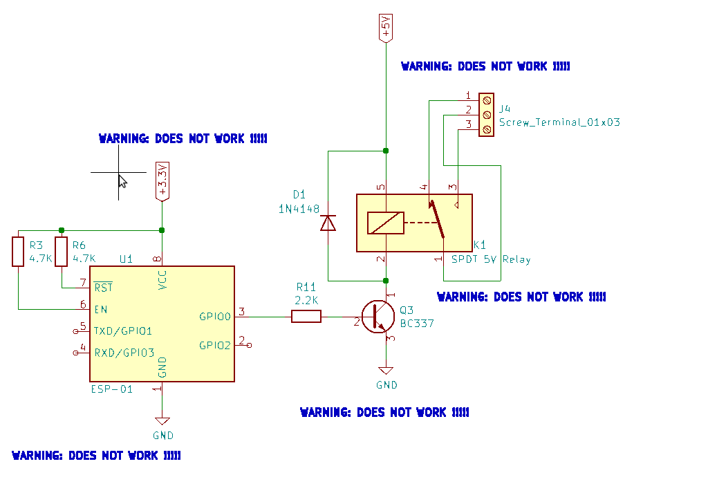
Pin GPIO0 needs to be in a HIGH state (that is, its voltage should be near Vcc) so that the stored program runs normally. If, for any reason, the voltage at the pin is at a level that is considered by the processor as logic LOW, the processor will enter flash mode. Therefore, in order to use the pin for our purposes, we must make sure that the voltage is logic HIGH at start-up. Control circuits that are based on a “positive” logic, such the one presented below, result in pulling the pin voltage to LOW and therefore are inappropriate. Please note that the circuit below DOES NOT WORK.
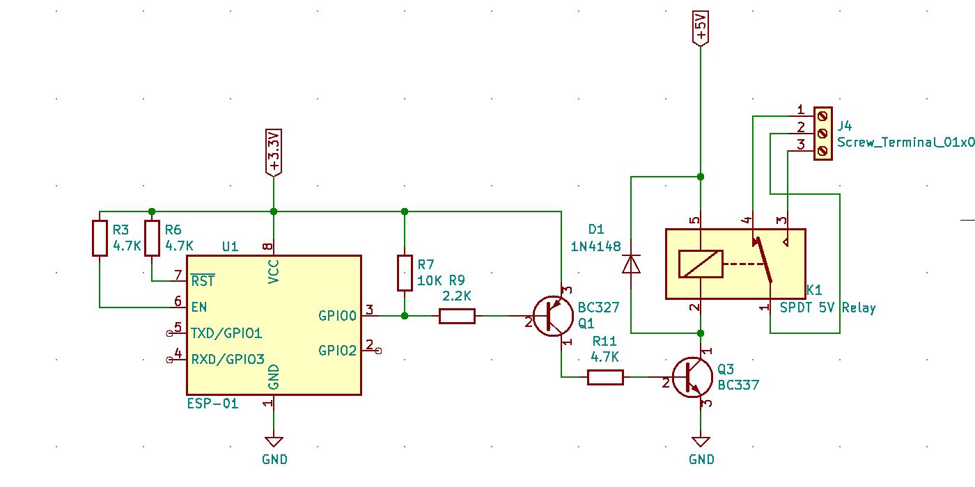
The solution is to implement a negative logic in our code. This means that HIGH voltage on the pin will signify an “Off” state, whereas a LOW voltage will be the “On” state. The circuit to implement this method employs a PNP transistor, followed by an NPN transistor. In this example circuit, a relay is driven by GPIO0. When we want to activate the relay, we write LOW to pin 0:
digitalWrite(0, LOW);
And when we want to de-activate the relay, we write HIGH.
digitalWrite(0, HIGH);
Because I try to write code that can be re-used in several projects, I introduce a constant such as gpioLogic and the code goes like:
/*
  Set true for a positive logic or false for a negative logic
*/
const bool gpioLogic = false;

void setup() {

...
   pinMode(2, OUTPUT);
....
}

void relayOn(int pin) {
  if (gpioLogic)
    digitalWrite(pin, HIGH);
  else
    digitalWrite(pin, LOW);
}

void relayOff(int pin) {
  if (gpioLogic)
    digitalWrite(pin, LOW);
  else
    digitalWrite(pin, HIGH);

}
Using two transistors instead of one, may be considered a burden. Yet, this implementation has the additional advantage of separating the power source of the processor from the power source of the load. It is easier to use relays, buzzers and other devices specified for use at 5V, 12V or higher, rather than at 3.3V. (Most of us have plenty of such equipment in our lab bins). Therefore, the momentary spikes in the supply voltage that are caused by the switching from on to off and vice versa, do not interfere with the processor.
The transistors are selected depending on the load consumption and the load operating voltage. The values of the resistors may be modified and optimised according to the current consumed by the load as well as the characteristics of the transistors.
A similar control circuit can be used with pin GPIO2, giving us one additional valuable pin.
Use case: Using pins TXD and RXD as I2C pins
Although pins TXD and RXD are mainly used as a serial interface, they are also general purpose I/O pins that can be programmed to operate as such. TXD is also referred to as GPIO1 and RXD as GPIO3. We must of course accept the fact that without a serial interface, we will be missing a way to communicate with our software and the main tool of debugging our code. Therefore, we need to be extra cautious and devise other ways of operating in the blind. But this is a huge subject and out of the scope of this article.
Using the pins as general purpose I/O is not trivial, because we must consider that when the chip restarts, it might try to communicate with the world using the pins in their normal function as TXD and RXD. Although they use the same chip, various firmwares or even versions of such firmwares behave in different manners. Therefore, consult the documentation (both chip data-sheet and firmware manuals) and experiment extensively, making good use of your lab instruments (oscilloscopes, digital analysers etc).
One way I have found to work with stability is to utilize this pair of pins in order to communicate with I2C devices, such as sensors, A/D converters, etc. We could even connect I/O port expanders such as PCF8574, but that would go beyond the limits of the ESP-01 and an ESP-12E or better module would be more appropriate. But, if we had a single sensor and/or a display such as a SSD1306 based OLED display, using TXD and RXD as I2C could be a nice solution.
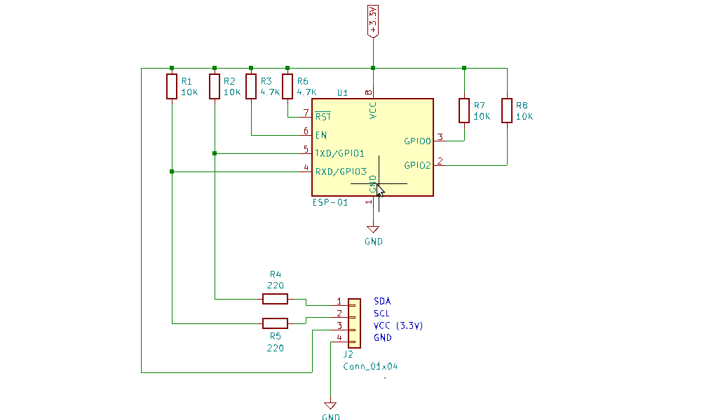
See the circuit below. The series resistors provide some safety from short-circuiting a pin in case both sides operate as outputs, before our code takes over.
In terms of software, in order to force pins TXD/GPIO1 and RXD/GPIO3 to operate as I2C pins functioning as SDA and SCL respectively, we must set in our code:
Wire.begin(1, 3)
The syntax is:
Wire.begin(sda_pin, scl_pin).
Conclusion
I have presented ways to exploit an ESP-01 as much as possible and utilize all four available GPIO pins. The above methods can mostly be utilized in hobby projects, due to dangers of frying the pins. For more serious or commercial projects, it will be better to select another more suitable module.
Have fun…


